Back Back
HAREM: High Aspect Ratio Etching and Metallization
( Former project )E. Sarajlic, C. Yamahata, M. Cordero, D. Collard, H. Fujita
Get the pdf file  Keywords: HAREM, SCREAM, Bulk micromachining, High Aspect Ratio, MEMS, Silicon, Microtweezers |
|
|
|
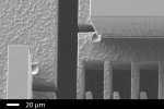
SEM micrograph of a prototype fabricated with the HAREM process
|
|
|
|

We have developed a simple bulk micromachining method for the fabrication of high aspect ratio monocrystalline silicon MEMS (MicroElectroMechanical Systems) in a standard silicon wafer. We call this two-masks microfabrication process HAREM, which is an acronym for High Aspect Ratio Etching and Metallization: it combines double-side etching and metallization to create suspended micromechanical structures with electrically 'insulating walls' on their backside. The insulating walls ensure a proper electrical insulation between the different actuation and sensing elements situated on either fixed or movable parts of the device.
To demonstrate the high potential of this simple microfabrication method, we have designed and characterized electrostatically actuated microtweezers that integrate a differential capacitive sensor. The prototype showed an electrical insulation better than 1 GΩ between the different elements of the |
|
device. Furthermore, using a lock-in amplifier circuit, we could measure the position of the moving probe with few nanometers resolution for a displacement range of about 3 µm.
This work was presented at the IEEE MEMS 2008 conf. and is published in the journal J. Micromech. Microeng. (DOI: 10.1109/MEMSYS.2008.4443656).
 |
HAREM micromachining process used for the fabrication of silicon tweezers.
This video was presented at the 21st IEEE Int. Conf. on Microelectromechanical Systems, MEMS 2008 (Tucson, Arizona, USA, January 13-17, 2008).
|
|
|
Back
Last modified: October 1st, 2009
|